The University of Tokyo School of Engineering Institute of Engineering Innovation
Research
We research the atomic structure/electric state and the generation mechanisms of materials properties in local structures, such as interfaces, surfaces and dislocations. Furthermore, we aim to construction the theory necessary for designing new materials. The following are representative of our research subjects.
Investigating the atomic structure/electric state and property generation mechanisms in grain boundary of ceramics
Ceramics are usually used in polycrystalline form, the properties of which are closely related to the internal grain boundaries. In this study, to investigate the correlation between grain boundary structure and functional properties, we seek to construct the theory for designing new materials. Our approach for investigating complicated sub-nanoscale grain boundary structure involves three main steps. [1] Fabrication and evaluation of the single grain boundary by the bicrystal method. [2] Direct observation of atomic structure of the grain boundary by transmission electron microscopy with sub-angstrom resolution. [3] Theoretical prediction of atomic structure/electric state by ab-initio calculations. Targeted materials are Al2O3, ZrO2, SrTiO3 and TiO2.
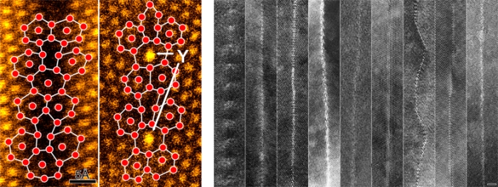
Left image:STEM images an Al2O3 grain boundary showing the presence of yttrium (J.P. Buban et al. Science 311, 212-215 (2006).
Right image:HRTEM images of tilt controlled ZrO2 grain boundary (N. Shibata et al. Phil. Mag. 84, 2381-2415 (2004).
Creating new nanowire devices using dislocations
Dislocations are atomic scale 1D defects in the crystal lattice, and play an important role in determmining mechanical properties. We research the fabrication of nanowire devices using dislocations in sapphire.
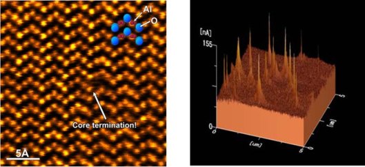
Left image:STEM image of dislocation core in sapphire. (N. Shibata et al. Science 316, 82-85 (2007).
Right image : High electric conductivity of Ti doped dislocations in sapphire.(A. Nakamura et al. Nature Materials 2, 453-456(2003).
Atomic structure/electric state analysis of heterointerfaces
Metal/ceramic composite materials play an important role in advanced technology, such as solid/oxide fuel cells, electrical devices and catalysts. The properties of composite materials depend considerably on the interface (heterointerface) which is formed by “metallic bonding” and “ionic bonding”. We use the effective methods of HRTEM observation and ab initio calculations to investigate the property-generation mechanism due to the metal/ceramic heterointerface.
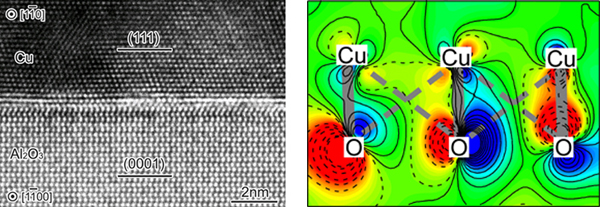
Left image : HRTEM image of Cu/Al2O3 interface, Right image : Chemical bonding mapping
T. Mizoguchi et al. Phys. Rev. B 74, (2006) 235408-1-10.
K. Matsunaga et al. Phys. Rev. B.74 (2006) 125423-1-8.
Ultimate analysis = Scanning transmission electron microscopy (STEM) and Electron energy loss spectroscopy (EELS)
Electron energy loss spectroscopy (EELS) in scanning transmission electron microscopy with sub-Å (0.01nm) resolution reveals the atomic structure/electric state of an atomic column. We apply the “Ultimate analysis” to dislocations, grain boundaries and heterointerfaces, and research the property-generation mechanisms in the local area.
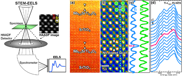
Left image : A schematic illustration of STEM-EELS
Right image : STEM-EELS analysis of SrTiO3/Nb-SrTiO3
(H. Ohta et al. Nature Materials 6, 129-134(2007), T. Mizoguchi et al. Phys. Rev. B. 77,24504-1-5(2008)).