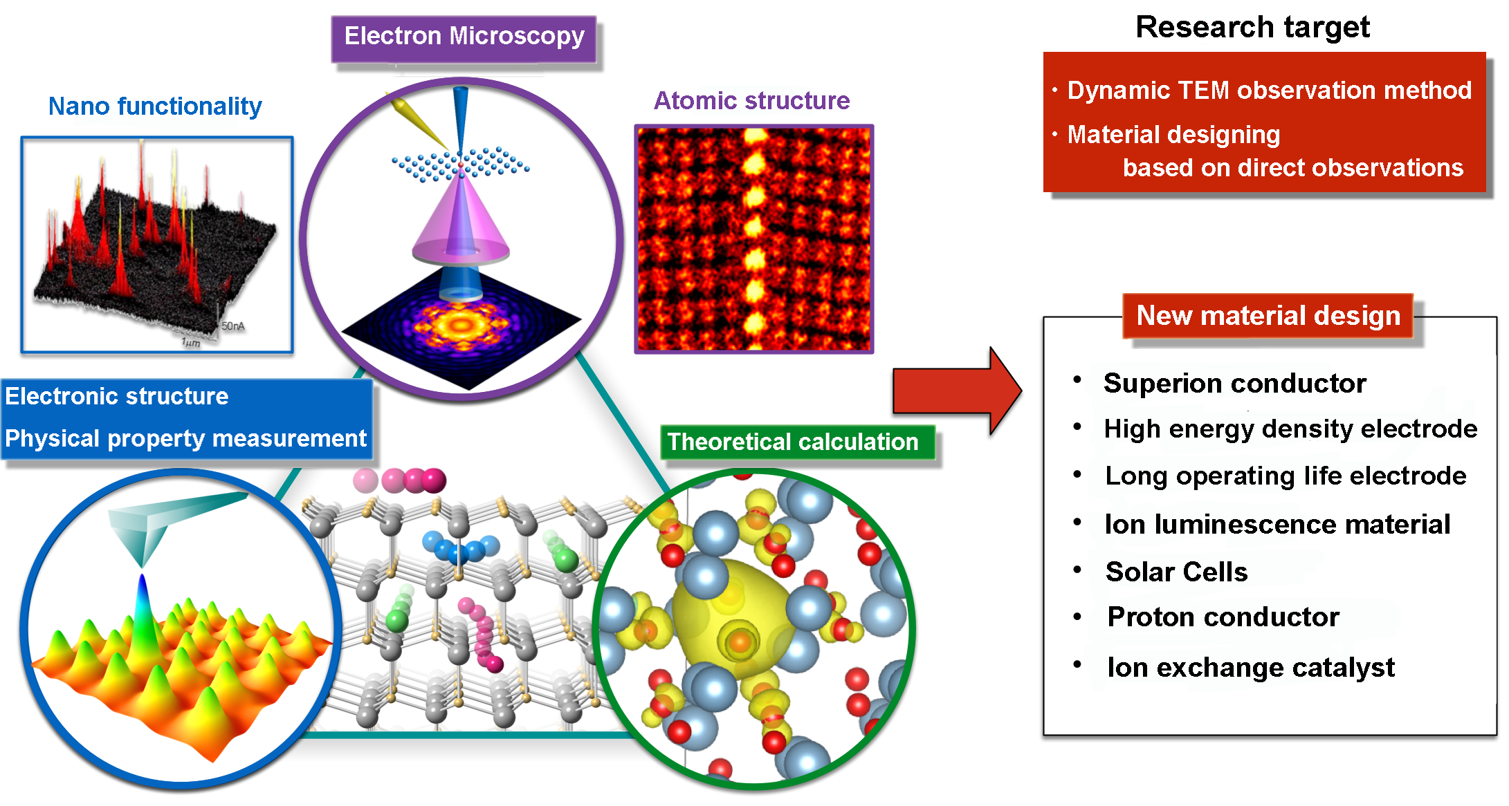

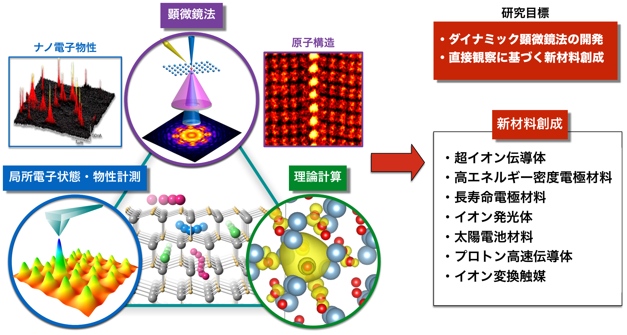
材料・デバイスのマクロな特性は、その内部に形成された界面、表面、点欠陥などのナノレベルの微細構造(ナノ構造)と密接に関連している。したがって、革新的な高機能・高性能材料を創出するためには、ナノ構造と機能発現の本質的メカニズムを解明し、その知見に立脚した材料設計を行う必要がある。材料内部に局在するナノ構造を解明するためには、原子分解能走査透過型電子顕微鏡(STEM)が非常に有効であるが、現状は静的な観察に留まっており、各種機能が発現するダイナミックな環境下での直接観察までには至っていない。
そこで本研究では、最先端原子分解能STEM法を、材料内部の超ミクロ現象の動的観察手法へと大きく進化させ、材料ナノ構造形成、機能発現の原子・イオンダイナミクスを可視化することを目指す。具体的には、構造材料、機能セラミックス、触媒、電池など、材料内部のナノ構造とそれに伴う原子・イオンダイナミクスが機能特性発現の鍵となる材料群を対象とする。これより、原子・イオンダイナミクスの超高分解能直接観察に基づくナノ構造設計・制御指針を確立し、新物質・新材料開発の基礎・基盤学理を構築することを最終的な目的とする。
研究の方法
原子・イオンダイナミクスの直接観察を行うためには、原子分解能STEMの時間分解能を飛躍的に向上させる必要がある。このため、電子プローブ高速スキャンシステムおよび高速電子検出システムを開発し、高速観察手法の確立を図る。また、実環境下にて発現する原子・イオンダイナミクスをSTEM内において再現するため、温度や荷重、電位といった試料環境が高度に制御できるその場観察用特殊試料ホルダーの開発を進める。開発の完了した装置を順次投入し、高空間・高時間分解能での原子・イオンダイナミクス観察を実施する。観察結果に基づいて、STEM分光法やプローブ顕微鏡を用いた局所物性測定、理論計算等を行い、原子・イオンダイナミクスと材料物性との相関性を明らかとする。上記手法を様々な材料系へ適用することにより、材料ナノ構造の原子・イオンダイナミクスの超高分解能直接観察に基づく物質・材料創成を目指す。
Purpose and Background of the Research
It is well known that nano-structures such as interfaces, surfaces, dislocations and point defects crucially determine the macroscopic properties of materials and devices. Thus, it is important to fundamentally understand the relationships between nano-structures and their properties, in order to create better and/or novel property materials and devices. Through advances in aberration correction technology over the last decade, scanning transmission electron microscopy (STEM) has achieved sub-0.5Å spatial resolution and it has become possible to directly characterize nano-structures inside materials at atomic dimensions.
However, the above atomic-resolution imaging methods are currently limited to image nano-structures in a stationary manner. To fundamentally and thoroughly understand the relationship between nano-structures and their properties, it is needed to observe nano-structures dynamically, i.e. when they actually exhibit their functional properties. In particular, atom and ion dynamics around nano-structures will be the key to understand the properties of many materials and devices. However, it is still a major challenge to realize atomic-scale dynamic observations of nano-structures inside materials under working conditions.
Research Methods
In this project, we divide our research plan into three main parts. The first part is the development of direct and dynamic imaging techniques of atoms and ions inside materials based on aberration-corrected STEM. The second part is the application of the newly developed atomic-resolution dynamic imaging techniques to actual materials science and engineering problems. In the third part, we develop better and novel property materials based on the design and control of local atom and ion dynamics around nano-structures.