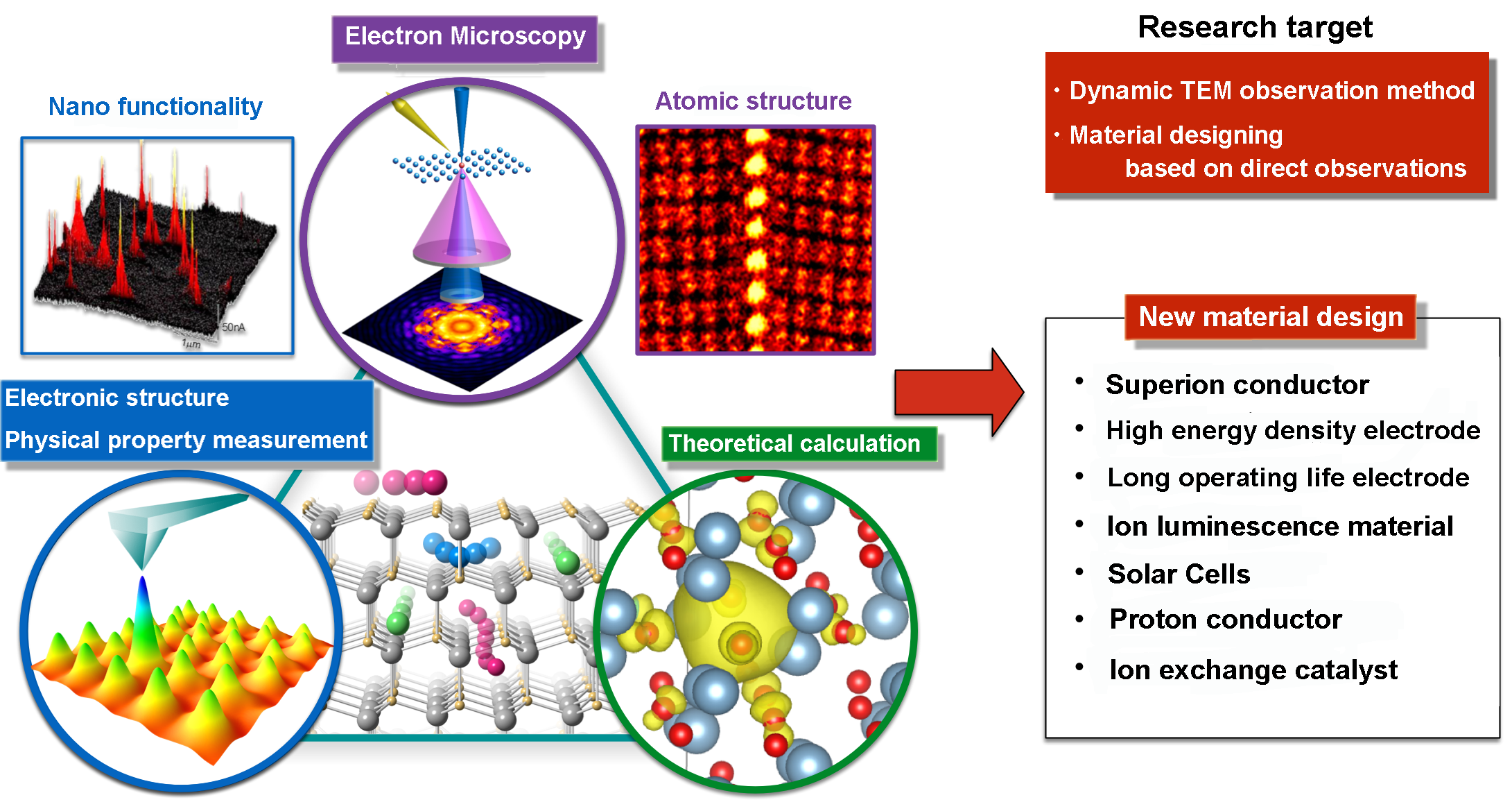

It is well known that nano-structures such as interfaces, surfaces, dislocations and point defects crucially determine the macroscopic properties of materials and devices. Thus, it is important to fundamentally understand the relationships between nano-structures and their properties, in order to create better and/or novel property materials and devices. Through advances in aberration correction technology over the last decade, scanning transmission electron microscopy (STEM) has achieved sub-0.5Å spatial resolution and it has become possible to directly characterize nano-structures inside materials at atomic dimensions.
However, the above atomic-resolution imaging methods are currently limited to image nano-structures in a stationary manner. To fundamentally and thoroughly understand the relationship between nano-structures and their properties, it is needed to observe nano-structures dynamically, i.e. when they actually exhibit their functional properties. In particular, atom and ion dynamics around nano-structures will be the key to understand the properties of many materials and devices. However, it is still a major challenge to realize atomic-scale dynamic observations of nano-structures inside materials under working conditions.
Research Methods
In this project, we divide our research plan into three main parts. The first part is the development of direct and dynamic imaging techniques of atoms and ions inside materials based on aberration-corrected STEM. The second part is the application of the newly developed atomic-resolution dynamic imaging techniques to actual materials science and engineering problems. In the third part, we develop better and novel property materials based on the design and control of local atom and ion dynamics around nano-structures.