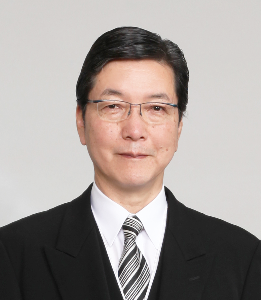
Yuichi Ikuhara, Professor
The University of Tokyo

Our project “Atom-by-atom imaging of ion dynamics in nano-structures for materials” has started from 2017, supported as a Grant-in-Aid for Specially Promoted Research of Japan Society for the Promotion of Science. On behalf of the project leader, it is my great honor to express my appreciation here.
Our project targets on materials, which is the key technology for the field of environment and energy, social infrastructure and information applications. Most of the materials in practical use are in the form of polycrystalline, so that grain boundaries (GBs) inevitably exist inside and significantly affect the macroscopic properties of these materials. GBs are composed of periodic structural units, of which the atomic arrangement largely differs from those inside the bulk. It is known that ionic conductivity can be realized along GBs, dopant segregation strengthens the mechanical properties of structural materials, and GBs in thin films often influence the electrical conductivities. Since the GB atomic structures greatly affect the functionalities, it is necessary to reveal the local structure-property relationships in these GBs at atomic scale, which requires electron microscopies with high spatial resolution.
In recent years, there has been a significant breakthrough in the field of the electron microscopies. That is, scanning transmission electron microscopy (STEM) combined with spherical-aberration correction technologies. Thanks to the aberration correction technology, the electron beam can be converged below 1 Å, and it is possible to directly visualize the atoms with that resolution. We are the first group to introduce this technique in Japan. In addition to the local structural analysis for materials science, we achieved 45 pm spatial resolution in 2014, and made a world record of 40.5 pm. In 2009, we developed annular bright-field (ABF) STEM method with JEOL Ltd and Japan Fine Ceramics Center(JFCC), which enables the first direct imaging of light elements of Li and H. Furthermore, it is now possible to visualize the local electric/magnetic field. When there is electric field inside material, electron beam would be deflected, and our group has developed a new segmented-type detector which enables to precisely measure such small deflections. This technique brought new breakthrough in the field of nano-characterization, and we successfully visualized the electric field even inside single atoms.
However, there is still a big challenge to resolve. That is, almost all the above atomic-resolution characterization methods are limited to the stationary imaging. In order to fundamentally and thoroughly understand the relationship between local nano-structures and their properties, it is necessary to carry out dynamical observations under working condition, especially atom and ion dynamics under the condition when they actually exhibit their functional properties. For example, if we can directly visualize the ion diffusion under electric field at high temperatures and identify the ion diffusion paths, it is possible to design superionic conductor; If we can directly visualize the crack propagation process under load, it is possible design high mechanical strength materials; If we can directly visualize the active site under catalytic atmosphere, it may design high performance catalyst.
The purpose of the present project is to develop atomic-resolution imaging techniques for atom and ion dynamics inside materials, by further improving spatial and time resolution and controlling the temperature, electric field, stress, and atmosphere. For example, by direct observation of the ionic conduction under electric field, and direct observation of the microscopic deformation process under load, we aim to fundamentally understand the relationships between nano-structures and functional properties. Through such direct imaging of atom/ion dynamics and fundamental understanding, we wish to establish new material design strategies, and therefore, contribute to the future materials innovation. Our project is currently run by the members from the University of Tokyo and Nagoya University, and we do look forward to your kind advices and supports.
2017 summer

